Silicon Wafer Inspection
Examine wafers for cracks, edge damage, inclusions, contamination and internal non-uniformities that may be difficult to distinguish with visible illumination.

Non-Destructive Wafer, Die and Package Inspection
Reveal cracks, voids, bonding defects, alignment errors and internal structures that may be hidden from visible cameras. Pembroke Instruments supplies high-resolution InGaAs SWIR cameras, microscope systems, optics and application guidance for silicon wafer inspection, advanced packaging and failure analysis.
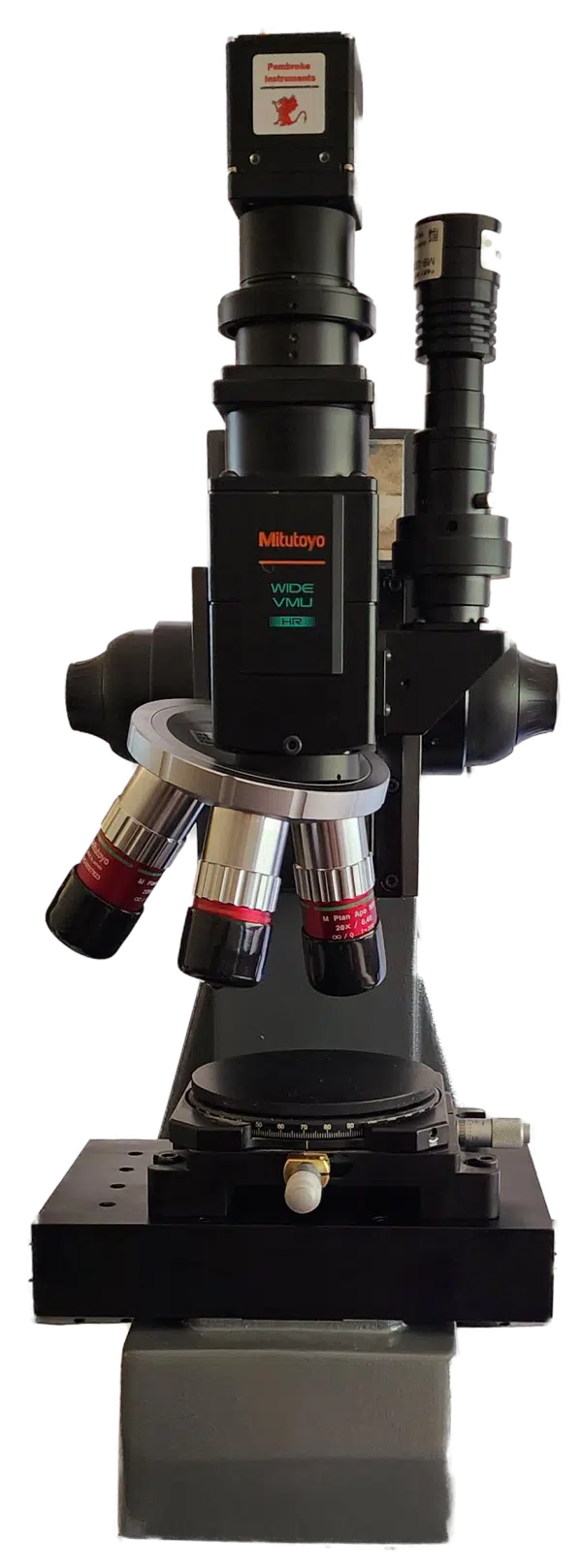
Configurable SWIR microscope platform for wafer, die, MEMS and package inspection.
Why Visible Imaging Is Not Enough
Semiconductor defects are frequently located below a wafer surface, inside a die, at a bonded interface or within an assembled package. Conventional visible cameras are limited because silicon strongly absorbs visible light. At suitable short-wave infrared wavelengths, silicon becomes substantially more transmissive, allowing an InGaAs SWIR camera to image structures and defects that are otherwise obscured.
SWIR imaging can therefore support non-destructive inspection without cutting, polishing or sectioning the sample. Depending on sample thickness, doping, metallization, surface treatment, wavelength and illumination geometry, the system can reveal subsurface features with useful contrast for research, process development, incoming inspection and production quality control.
The illumination wavelength, lens transmission, magnification, working distance, field of view, sample orientation, exposure time and image processing all affect the final result. Pembroke can help define the complete imaging configuration.
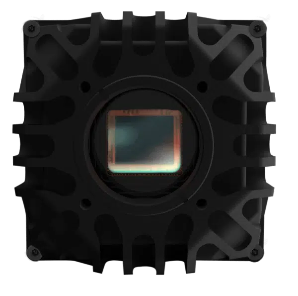
Megapixel SWIR cameras provide greater inspection detail, a larger field of view, or fewer camera positions than conventional VGA-format systems.
View SenS 1280Primary Applications
A properly configured SWIR system can support inspection from full wafers and production lines down to microscope fields of view for localized defect analysis.
Examine wafers for cracks, edge damage, inclusions, contamination and internal non-uniformities that may be difficult to distinguish with visible illumination.
Image through silicon to examine structures, locate suspect areas and support non-destructive failure analysis before destructive cross-sectioning.
Detect voids, trapped particles, air gaps, incomplete bonding and alignment problems between silicon layers or bonded substrates.
Inspect alignment, internal package features and selected defects in assemblies where visible access is blocked by silicon or other package components.
Investigate internal microstructures, through-silicon vias, channels, cavities and bonded interfaces using microscope optics and controlled SWIR illumination.
Identify cracks and process defects in silicon photovoltaic materials and panels using high-resolution SWIR imaging and application-specific illumination.
Defect Detection
Actual detectability varies with the sample and optical setup, but SWIR imaging is commonly evaluated for the following conditions:
Semiconductor materials and package designs vary. For best results, provide Pembroke with the sample type, silicon thickness, approximate defect size, desired field of view, inspection speed and any existing illumination constraints.
We can help determine whether a standard 900-1700 nm InGaAs camera, a microscope system, a high-resolution sensor or another configuration is most appropriate.
Camera Selection
Resolution is important, but it must be balanced with sensitivity, frame rate, exposure time, field of view, interface, optics and available illumination.
| Inspection Requirement | Recommended Starting Point | Why It Fits | Pembroke Resource |
|---|---|---|---|
| Highest area-scan image detail | SenS 1920, 1920 × 1080, 8 µm pixels | Supports larger fields of view, finer spatial sampling and detailed wafer or die inspection. | SenS 1920 details |
| High resolution in a compact format | SenS 1280, 1280 × 1024, 10 µm pixels | Strong balance of spatial detail, sensitivity, compact size and interface flexibility. | SenS 1280 details |
| High speed or compact machine vision | SenS 640V-ST family | TE-cooled VGA format with fast acquisition, triggering and practical OEM integration options. | SenS 640V-ST details |
| Long exposure or low available light | SenS HiPe | Designed for long-exposure, low-noise imaging where signal levels are limited. | SenS HiPe details |
| Micron-scale field of view or high magnification | Configured SWIR microscope | Combines camera, objectives, illumination, filters, stable focus and sample positioning. | SWIR microscope options |
Final model selection should be confirmed against current specifications and the actual inspection geometry. Pembroke Instruments can help compare cameras and calculate pixel sampling within the required field of view.
Featured Solutions
Full-HD, 2-megapixel InGaAs SWIR camera for high-resolution inspection.
High-definition SWIR camera for wafer inspection, microscopy and machine vision.
Custom systems for wafer, die, MEMS, TSV and bonded-interface inspection.
Build the Complete Inspection System
Define the smallest crack, void, particle or alignment error that must be detected. This drives the required optical resolution and pixel sampling.
State whether the system must inspect a full wafer, a die, a package region or a microscope-scale area. Field of view strongly affects lens choice and detail.
Select illumination according to silicon thickness, sample construction, transmission or reflection geometry, contrast and detector sensitivity.
Production-line inspection may require short exposures, triggering, ROI, selective line readout or high-frame-rate acquisition.
Confirm working distance, sample clearance, lens mount, microscope objective, motion stages and whether the camera must fit an existing machine.
Define USB3, Camera Link, GigE, CoaXPress or other integration needs, plus GUI, SDK, GenICam, triggering, LabVIEW, MATLAB or custom software requirements.
Pembroke Application Support
Pembroke Instruments can help you evaluate camera resolution, pixel size, sensitivity, cooling, optics, illumination, field of view, working distance, triggering, software and mechanical integration. For microscope applications, we can configure the camera, objective, zoom optics, filters, stand and sample positioning as a complete system.
Frequently Asked Questions
Silicon becomes increasingly transmissive at suitable near-infrared and SWIR wavelengths, allowing an InGaAs camera to image selected structures and defects beneath the surface. Results depend on wavelength, silicon thickness, doping, surface condition, metallization, illumination and optical geometry.
Common uses include silicon wafer inspection, crack detection, wafer bonding analysis, die and package inspection, alignment checks, MEMS and TSV analysis, solar-cell inspection and non-destructive failure analysis.
Visible cameras mainly show surface features because silicon absorbs visible light. SWIR imaging can provide subsurface information and contrast through silicon, enabling detection of defects or structures that visible cameras cannot see.
Depending on the sample and setup, SWIR systems may reveal cracks, voids, contamination, trapped particles, bonding defects, internal structures, interface separation and package or wafer alignment errors.
Resolution should be selected from the required field of view and smallest detectable feature. A 2 MP SenS 1920 or 1.3 MP SenS 1280 can provide more spatial detail than VGA cameras, while microscope optics may be needed for localized micron-scale inspection.
Not always. Strong illumination, short exposures and wider fields of view may work with uncooled or moderately cooled cameras. Low-light, long-exposure or high-magnification applications often benefit from TE cooling and lower dark signal.
Yes. Camera families are available with machine-vision interfaces, triggering, ROI functions, SDKs and integration options. The correct configuration depends on line speed, exposure time, synchronization, field of view and processing needs.
Yes. Pembroke can configure SWIR microscope systems around required field of view, magnification, working distance, illumination, camera sensitivity, filters, stand stability, sample stages and software workflow.
Request Technical Guidance or Pricing
For a practical recommendation, include as much of the following information as possible:
Pembroke Instruments will review the application and recommend a suitable SWIR camera, lens, microscope or integration approach.
Send in your requests for informaation