PCB & Electronics Testing
Locate overheating components, short circuits, leakage paths, high-resistance connections and unexpected power dissipation across operating circuit boards.

Semiconductor, PCB & Electronics Failure Analysis
Use two complementary imaging methods to answer two different failure-analysis questions: What is hidden beneath the surface? and Where is electrical energy becoming heat? Pembroke Instruments supplies SWIR microscope solutions for through-silicon and subsurface inspection, plus thermal microscope systems for localized temperature mapping of powered electronics.
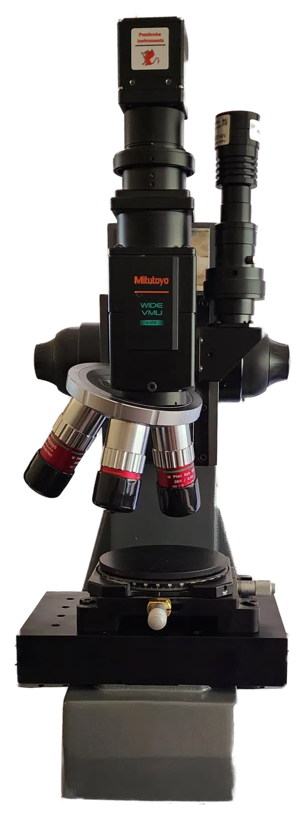
Configurable SWIR microscope platform for wafer, die, MEMS, bonded-interface and package inspection.
Two Imaging Modes, Different Information
Visible microscopy is often the starting point, but it cannot provide every answer. SWIR and thermal microscopy extend inspection in different directions: SWIR can reveal selected subsurface structures through silicon, while thermal imaging converts temperature distribution into a spatial map of circuit or device behavior.
Silicon strongly absorbs visible light but becomes substantially more transmissive at suitable near-infrared and SWIR wavelengths. With appropriate optics and illumination, InGaAs SWIR cameras can support non-destructive inspection of structures and defects that may be hidden beneath the surface.
A thermal microscope shows temperature distribution rather than visible structure. On powered boards and devices, it can quickly identify abnormal heating and guide electrical probing or deeper failure analysis toward the most likely problem area.
Thermal Microscope Spotlight
Thermal microscopy adds quantitative temperature information to small-area inspection. Instead of showing only physical structure, it maps where heat is generated, how it spreads, and how a device changes as power, load or operating conditions change.
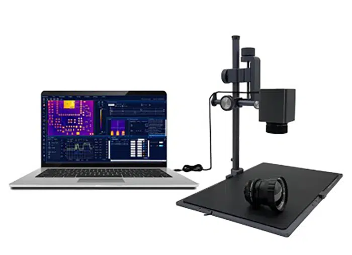
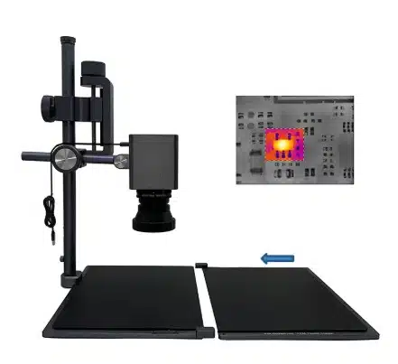
Pembroke Instruments can configure a complete thermal microscope system around the sample and test requirement. A typical platform combines a 640 × 512 LWIR thermal camera, macro or microscope optics, vertical mounting, a sample translation stage, an optical breadboard and radiometric analysis software.
Expanded Thermal Microscopy Applications
Thermal microscopy is useful whenever a small heat source, gradient or transient temperature change provides a clue to performance, manufacturing quality or failure mechanism.
Locate overheating components, short circuits, leakage paths, high-resistance connections and unexpected power dissipation across operating circuit boards.
Identify localized heating, leakage current, package-related thermal behavior and temperature non-uniformity in ICs and semiconductor devices.
Analyze heating in power devices, regulators, MOSFETs, connectors and thermal-management structures under controlled load conditions.
Look for hot spots, shunts, non-uniform heating and other thermal signatures associated with defective photovoltaic cells and materials.
Measure thermal behavior in coatings, films, composites, microstructures and phase-change materials where conventional thermal cameras lack enough spatial detail.
Evaluate absorption-induced heating, optoelectronic components, laser-exposed materials and package-level thermal effects.
Complete Thermal Microscope Configuration
A microscope application cannot be specified from sensor resolution alone. Sample size, target feature size, working distance, optics, stage geometry, temperature range and analysis workflow all determine whether the system will resolve the thermal behavior that matters.
For the fastest application review, provide the sample dimensions, smallest hot spot or feature of interest, required field of view, available working distance, expected temperature range and whether the device will be powered during inspection.
If electrical data must be synchronized with the thermal measurement, include the voltage/current test workflow as well.
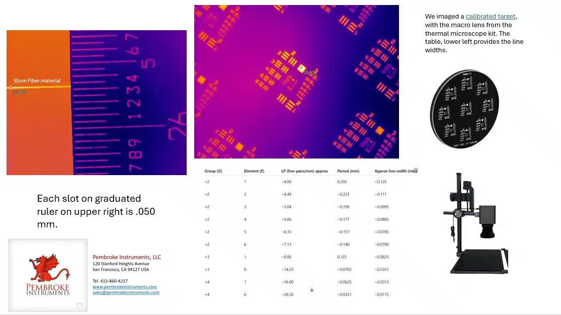
PCB and IC-level thermal detail: use calibrated targets and real device imagery to verify that the optics and field of view provide enough spatial resolution for the feature being investigated.
Technique Selection
| Inspection Question | Best Starting Technique | What It Can Add |
|---|---|---|
| Is there a crack, void, interface defect or structure beneath silicon? | SWIR microscopy | Non-destructive subsurface contrast through silicon at suitable wavelengths. |
| Which component or region is overheating on a powered PCB? | Thermal microscopy | Full-field visualization of localized temperature rise and thermal gradients. |
| Is a bonded interface aligned or complete? | SWIR microscopy | Inspection of selected bonded layers, air gaps, voids and alignment problems. |
| Is a suspect IC dissipating more power than expected? | Thermal microscopy | Comparison of heating behavior under startup, idle or controlled load. |
| Do I need to correlate an internal feature with abnormal heating? | Use both | SWIR provides structural information; thermal microscopy provides operating temperature behavior. |
| Where should I probe electrically or inspect more closely? | Thermal first, then targeted inspection | Thermal imaging can identify where to look first; SWIR or visible microscopy can then examine structure at that location. |
Primary Applications
Inspect wafers and dies for cracks, edge damage, selected internal non-uniformities and structures that may be obscured in visible imaging.
Investigate bonded interfaces, voids, air gaps, channels, cavities, alignment and through-silicon structures using microscope optics and controlled SWIR illumination.
Support non-destructive inspection of internal package features and selected defects where visible access is blocked by silicon or package construction.
Identify localized heating around ICs, regulators, MOSFETs, resistors, connectors, traces and other board-level components.
Use abnormal or unexpected heating as a fast visual clue to electrical faults, excessive power dissipation or localized current paths.
Observe temperature response in semiconductor devices, LEDs, sensors, resistors, microelectronics and other components under controlled operating conditions.
See the Applications
Explore SWIR imaging for wafer, die, package and through-silicon inspection.
Visualize temperature distribution across PCBs, components, semiconductor devices and small samples during troubleshooting and failure analysis.
Combined Failure-Analysis Workflow
For complex semiconductor or electronics problems, a combined workflow can reduce trial-and-error by first locating the problem spatially, then examining the relevant structure or interface in greater detail.
Document the sample, suspected feature size, operating condition, required field of view and whether the issue is structural, thermal or both.
For powered electronics, thermal microscopy can identify hot spots, asymmetry, abnormal gradients or unexpected temperature rise.
Where silicon blocks visible access, use SWIR microscopy to examine selected subsurface features, interfaces, cracks, voids or alignment.
Use the imaging results to guide electrical measurements, component inspection, design changes, rework or deeper root-cause analysis.
Pembroke Microscopy Solutions
Custom microscope configurations for wafer, die, MEMS, TSV and bonded-interface inspection.
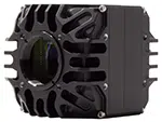
SenS 1920 and SenS 1280 cameras provide high spatial sampling for detailed inspection and microscope integration.
Configured LWIR microscope systems for quantitative temperature mapping of PCBs, ICs, semiconductor devices and small materials samples.
Define the Complete Imaging Requirement
For SWIR, wavelength, lens transmission, magnification, working distance, sample construction and illumination geometry affect contrast and detectability. For thermal microscopy, field of view, working distance, operating condition and the size of the thermal feature determine whether the measurement is useful. Pembroke can help define the complete imaging configuration rather than selecting a camera in isolation.
Pembroke Application Support
Pembroke Instruments can help evaluate resolution, field of view, pixel size, camera sensitivity, cooling, optics, illumination, working distance, magnification, filters, positioning, software and mechanical integration. The goal is to configure the imaging method around the inspection problem—not force the application around a camera specification.